

 388
388


Smart Wall Switch PCBA | Remote App & Scheduled Timer Control, Optimised For Real World Wall Box Installation
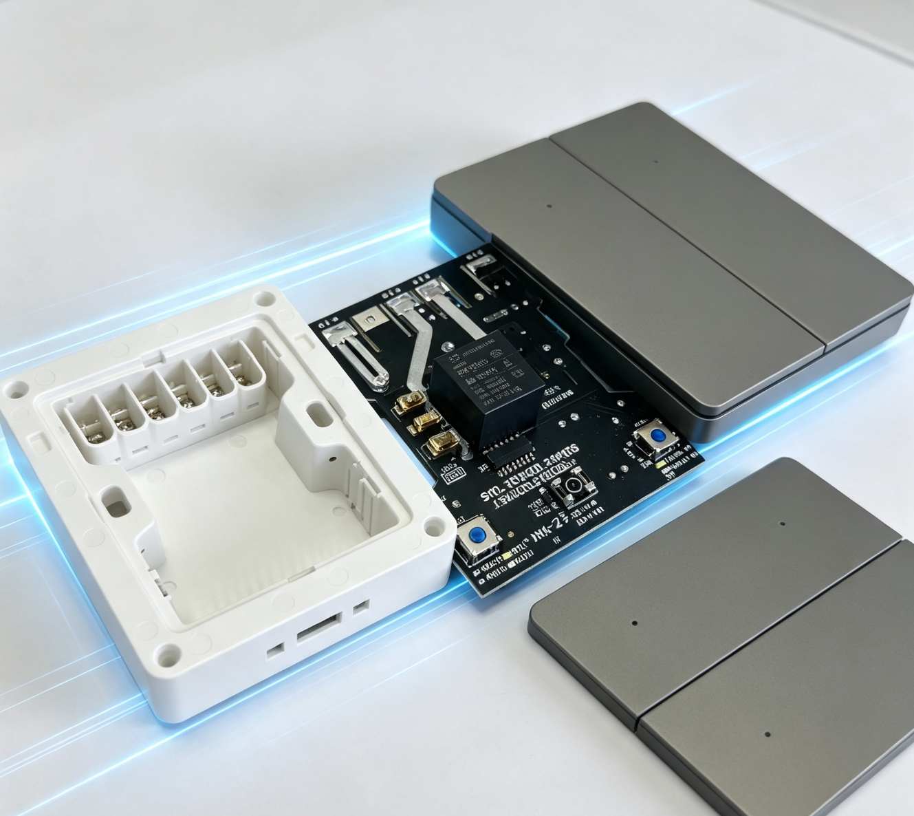
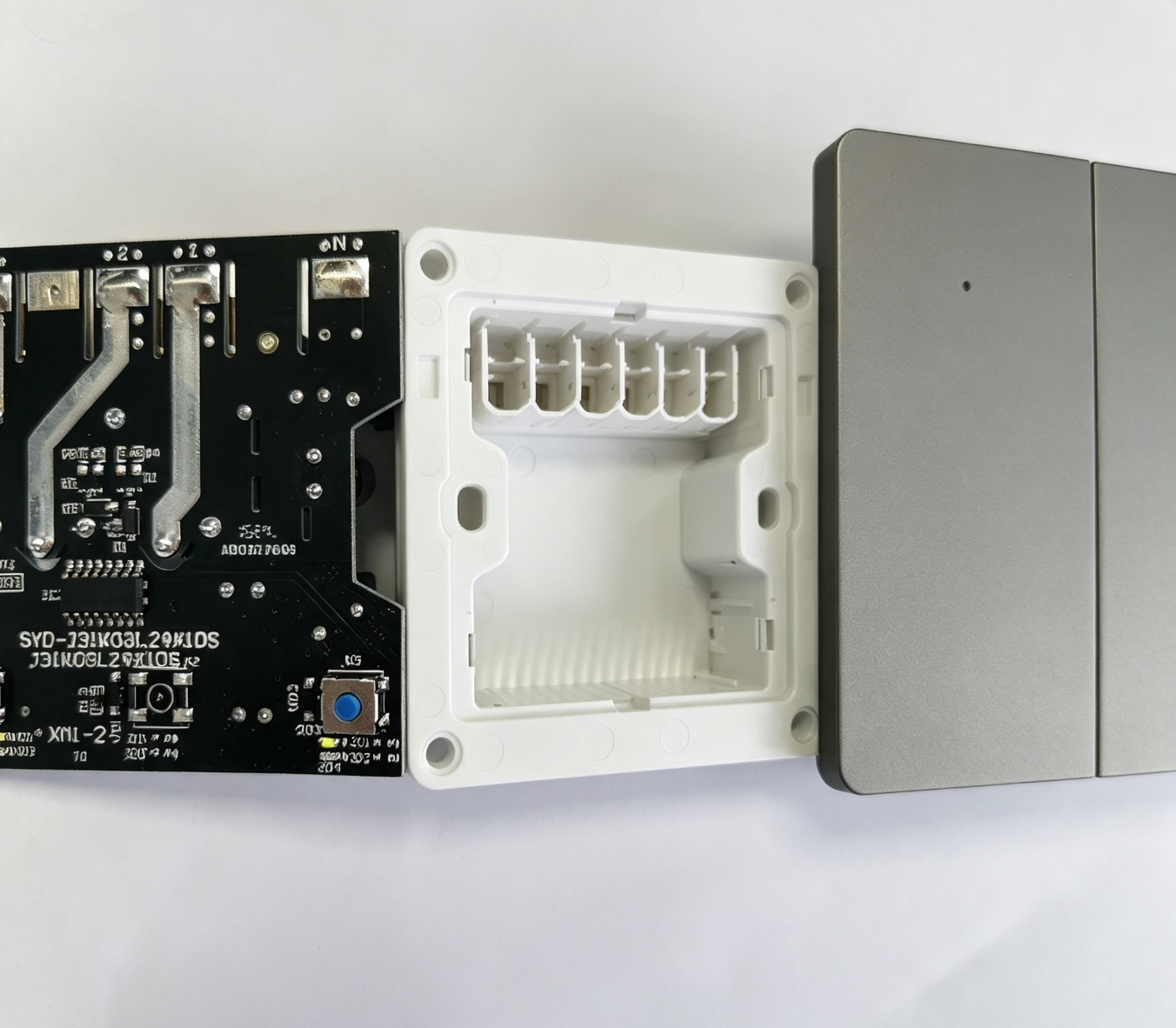
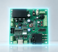
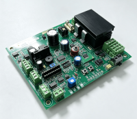
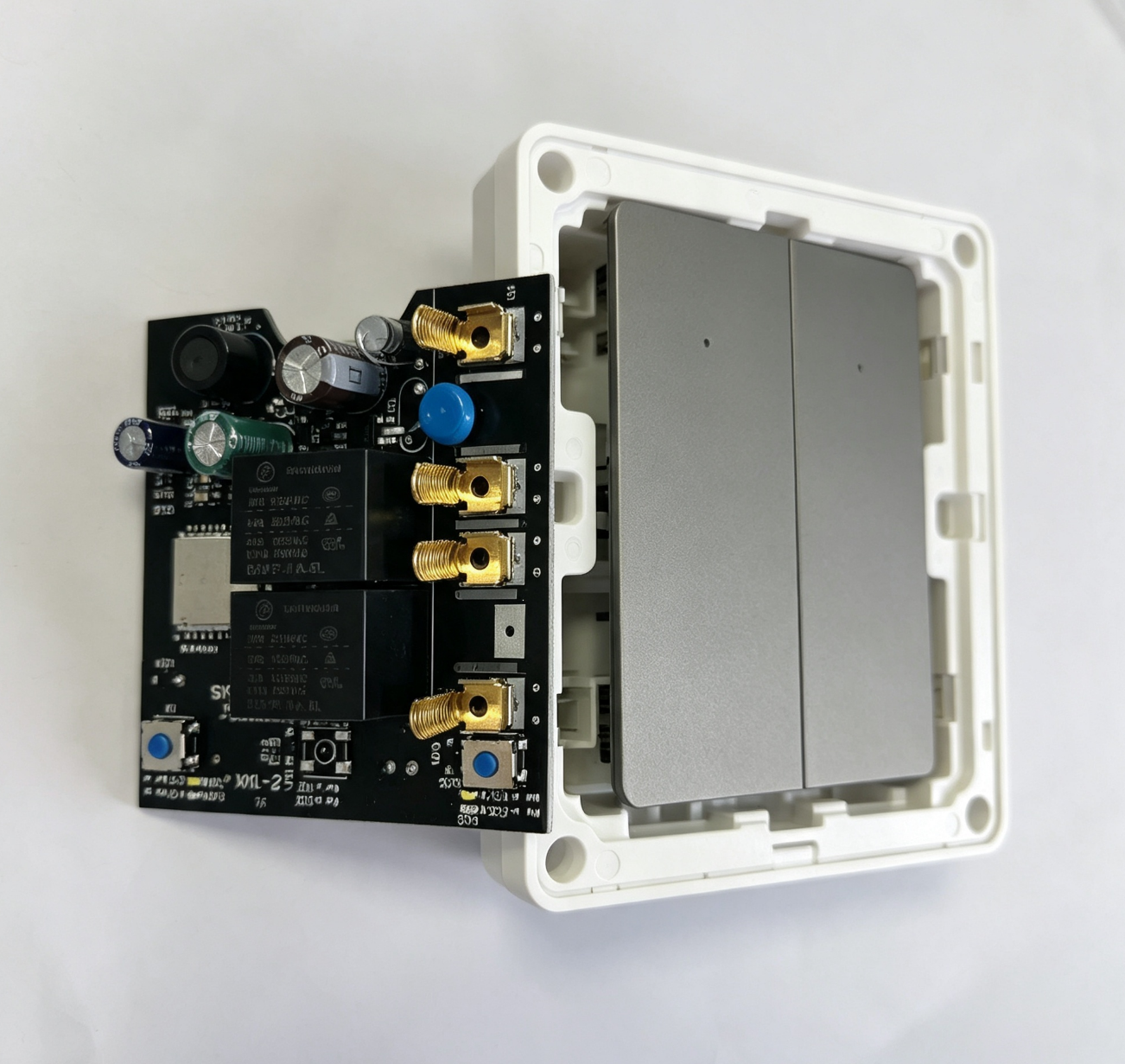
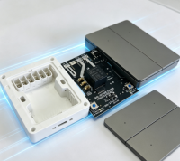
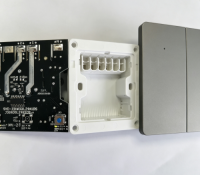
When we take on smart wall switch PCBA projects, most of the hard won adjustments stem from physical fitting constraints rather than wireless function debugging alone. A lot of incoming customers already own finished front panels and standard 86 type wall junction boxes, so we cannot start circuit layout without locking down mechanical boundaries first. The internal usable space inside a common 86 wall box is often tighter than datasheet parameters suggest, especially once pre installed house wiring is tucked inside. If we place tall electrolytic capacitors or relay components too close to PCB edges, installers will struggle to seat the full assembly; even if all electrical tests pass on the bare board, the finished unit may refuse to slide fully into the wall box during site installation. That is why we reserve clear edge clearance zones on the board outline early in layout phase, keeping high profile components set inward, away from board borders.
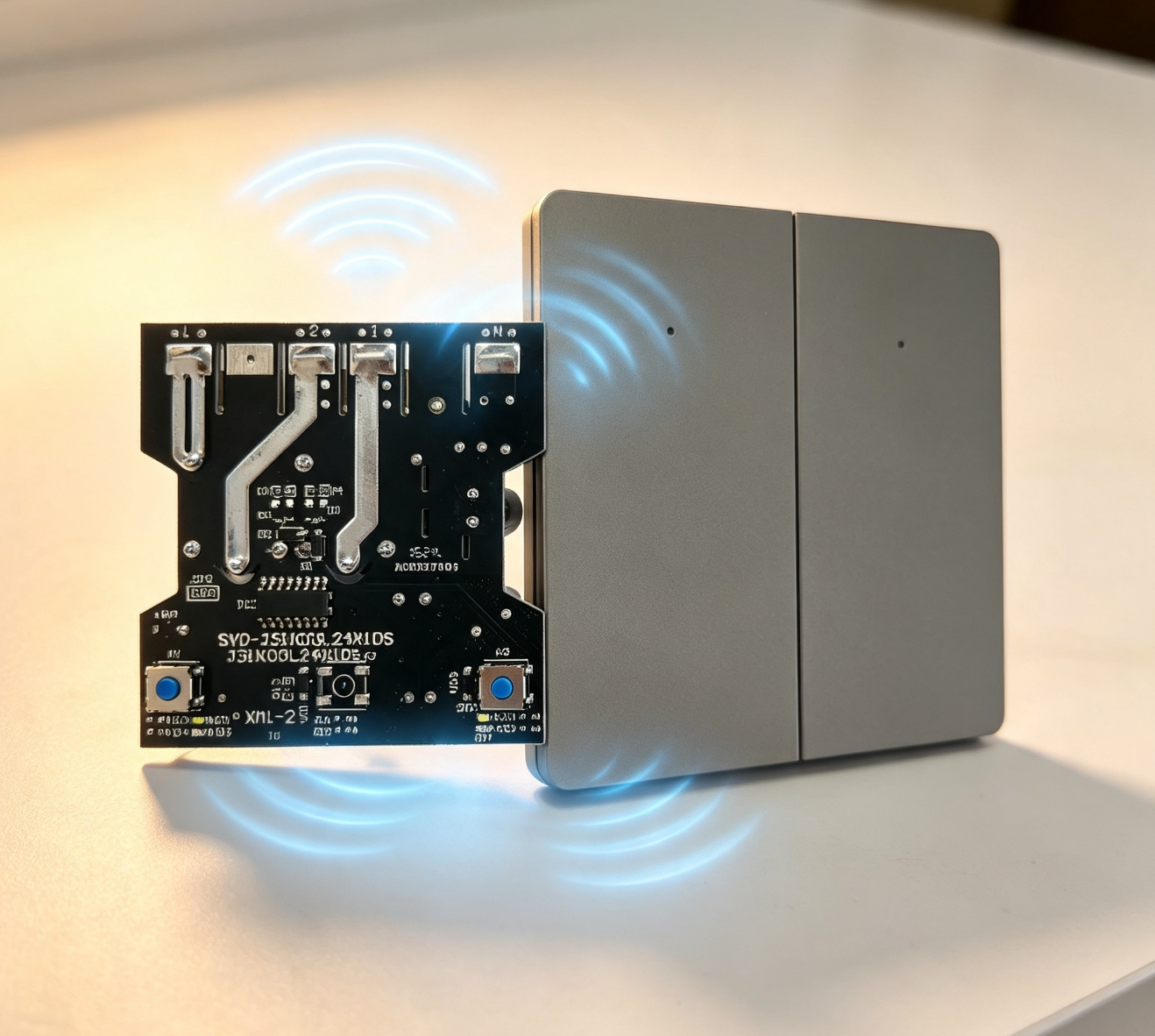
Screw hole positions demand careful cross checking as well. Many enclosure moulds have fixed mounting posts offset by less than one millimetre. Minor deviation in PCB mounting hole coordinates will mean installers cannot align screws through both plastic housing and circuit board. We regularly cross reference customer’s 3D enclosure files against our PCB footprint, rather than only working from written dimension lists. Terminal block layout is another frequent pain point encountered during real world fitting. Electricians on site need direct, unobstructed access for stripping and inserting live, neutral and load wires. When terminals are tucked beneath large relays or surface mount chips, wiring work slows down significantly, and accidental short circuit risks rise. We arrange power terminals toward one exposed board edge whenever possible, sorting terminal sequence to match regional wiring conventions, so field technicians do not need to cross over thick copper wires inside the confined box cavity.
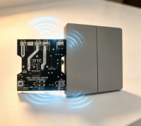
Wireless performance behaves differently under real installation versus bench lab conditions. Metal wall boxes, bundled household power cables and plaster wall material all attenuate radio signal. We have met prototypes that achieved flawless app response sitting on an open workbench, yet suffered delayed trigger commands or random offline status once fitted inside metal back boxes. Module placement becomes critical here; we shift the wireless chip away from heavy current relay copper traces which introduce electrical noise, and keep adequate separation between antenna tracks and high voltage power circuits. Standby current and wake up latency also cannot rely purely on simulation data. For mains powered smart switches, excessive quiescent draw adds up across dozens of household units. We run continuous ageing tests under actual enclosure thermal conditions, measuring real standby draw instead of only component theoretical values. Wake up time from low power sleep mode needs balancing too: too short and average standby power climbs, too long and end users notice lag after sending app remote commands or activating scheduled timer tasks.
Once layout revisions resolve mechanical and baseline electrical concerns, we move to limited trial batches, usually between 50 and 200 pieces. This small batch phase exists to catch issues software simulation and bare board testing cannot expose. During sample assembly, we check whether solder points stay clear when the board snaps into plastic housing, whether button tactile switches align perfectly with front panel push points, and whether LED indicator light leakage gets contained inside the panel cut outs. We also arrange mock site like testing: fit trial PCBA into genuine customer supplied back boxes, loop in same gauge household copper wiring installers will use on site, and run weeks of cyclic scheduled switching cycles. Quite often we find minor fix items at this stage, for example trimming a tiny section of PCB outline to clear an internal plastic rib inside the junction box, shifting one terminal position to avoid wire crowding, or fine tuning firmware sleep parameters to bring standby consumption down to acceptable range.
Jumping directly to mass production skipping this practical validation creates avoidable commercial risk. Lab validation can verify relay switching logic, app communication protocol and basic electrical safety, but it cannot fully replicate cramped wall box environments, messy field wiring conditions, long term thermal drift inside sealed enclosures. Every tweak derived from small batch physical fitting reduces rework rate once goods reach end market installers. Even with mature reference designs, we still insist on going through this physical fitting workflow for each new smart switch variant, as enclosure dimensional tolerance differences from different mould suppliers will introduce new fitting variables we cannot anticipate from drawings alone.
#smartwallswitchPCBA,#wallswitchboard,#wirelessswitchPCBA,#homeautomationPCBA,#highcurrentrelayPCBA,#remotescheduledcontrol,#appcontrolledswitch


Have a question or need a quote? Fill out this form and our team will get back to you quickly!